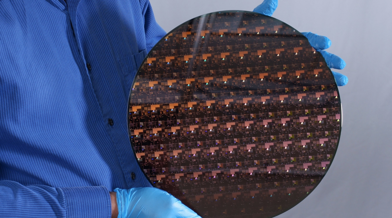
IBM’s Revolutionary 2nm Chip Uses Components Smaller Than a Strand of DNA
IBM
As phones and computer systems grow more demanding, makers are looking for powerful chips that utilize less energy. Now, IBM is giving us a look of the future with the worlds first 2nm chip, which boasts 45% much better higher efficiency and utilizes 75% less energy than the finest 7nm chips.
Developed simply four years after IBM revealed its 5nm chips, the new 2nm chip fits 50 billion transistors onto a wafer the size of a fingernail. Several of its parts are smaller than strands of DNA, thanks to the help of brand-new Extreme Ultra Violet (EUV) technology.
According to IBM, the new 2nm style might lead to phones with a four-day battery life, reduce the carbon footprint of data centers, increase the processing power of laptop computers, and unlock a new generation of AI.
Anyone acquainted with Apples transition to 5nm M1 processors understands that these very little, effective chips are innovative. Still, products with 2nm chips may not show up till 2027 (based upon an informed guess from Intel). By that time, consumers could currently grow used to 3nm and 5nm chips, so the advantages of 2nm might not be as apparent.
In any case, IBM wont be the one producing our 2nm chips. The computing giant is more of a research study laboratory nowadays, producing new innovation rather of offering products. IBMs partners, namely Samsung and Intel, will probably be the first to gain from this tech.
Source: IBM by means of Liliputing