IBM’s Revolutionary 2nm Chip Uses Components Smaller Than a Strand of DNA
IBM
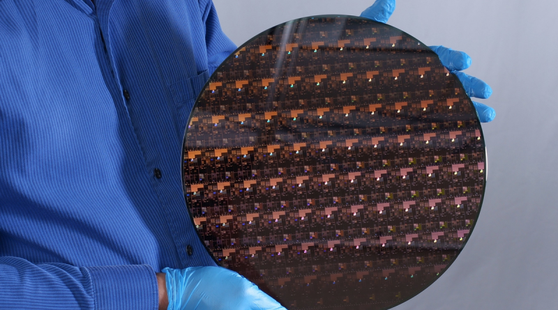
As phones and computer systems grow more demanding, makers are searching for effective chips that utilize less energy. Now, IBM is offering us a glance of the future with the worlds first 2nm chip, which boasts 45% better greater performance and utilizes 75% less energy than the very best 7nm chips.
Developed just four years after IBM announced its 5nm chips, the new 2nm chip fits 50 billion transistors onto a wafer the size of a fingernail. Several of its components are smaller sized than strands of DNA, thanks to the aid of brand-new Extreme Ultra Violet (EUV) innovation.
According to IBM, the new 2nm design could result in phones with a four-day battery life, decrease the carbon footprint of data centers, increase the processing power of laptops, and unlock a new generation of AI.
Anyone acquainted with Apples shift to 5nm M1 processors understands that these super little, effective chips are innovative. Still, products with 2nm chips may not get here until 2027 (based on an educated guess from Intel). By that time, consumers might currently grow used to 3nm and 5nm chips, so the benefits of 2nm may not be as obvious.
In either case, IBM will not be the one producing our 2nm chips. The computing giant is more of a research laboratory nowadays, producing new innovation rather of offering items. IBMs partners, namely Samsung and Intel, will probably be the very first to take advantage of this tech.
Source: IBM via Liliputing