IBM’s Revolutionary 2nm Chip Uses Components Smaller Than a Strand of DNA
IBM
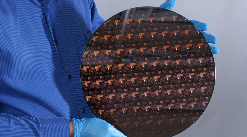
As computers and phones grow more requiring, makers are searching for powerful chips that use less energy. Now, IBM is providing us a glance of the future with the worlds very first 2nm chip, which boasts 45% better higher efficiency and uses 75% less energy than the finest 7nm chips.
Developed just 4 years after IBM announced its 5nm chips, the new 2nm chip fits 50 billion transistors onto a wafer the size of a fingernail. Numerous of its components are smaller sized than hairs of DNA, thanks to the aid of brand-new Extreme Ultra Violet (EUV) technology.
According to IBM, the new 2nm design could cause phones with a four-day battery life, minimize the carbon footprint of information centers, increase the processing power of laptops, and unlock a brand-new generation of AI.
Anybody knowledgeable about Apples transition to 5nm M1 processors understands that these very little, efficient chips are advanced. Still, products with 2nm chips may not arrive up until 2027 (based upon an educated guess from Intel). By that time, consumers might already grow used to 3nm and 5nm chips, so the advantages of 2nm might not be as obvious.
In either case, IBM wont be the one producing our 2nm chips. The computing giant is more of a research study lab nowadays, producing brand-new technology instead of selling items. IBMs partners, particularly Samsung and Intel, will probably be the very first to take advantage of this tech.
Source: IBM through Liliputing